Research Article | | Peer-Reviewed

Effects of Tin Doping Concentration on the Structural and Optical Properties of Cadmium Oxide Nanoparticles

Received: 23 May 2025     Accepted: 9 June 2025     Published: 30 June 2025
Views:       Downloads:
Abstract

Wet chemical process was successfully used to synthesize tin doped and undoped cadmium oxide nanoparticles. Cadmium acetate, sodium hydroxide, mercaptopropionic acid and tin chloride were used as starting materials for synthesizing the nanoparticles. The reaction was carried out in a single three-necked flask under reflux at 80°C for 2 hours and the solution was allowed to cool to room temperature. The precipitate was washed, dried, annealed and grounded to obtain the powder for further analysis. The phase and structure of the nanoparticles was studied using the X-ray diffraction equipment. Debye Scherrer’s equation was used to calculate the crystallite sizes of the doped and undoped nanoparticles. The XRD pattern displayed face centered cubic structure of cadmium oxide. When CdO was doped with Sn the intensity peaks decreased from 1650 a. u for pure CdO to 1235 a. u at 1% Sn doped and at 3.5% Sn doped, the intensity peak was 239 a. u. Increase in the doping concentration resulted in significant increase in grain size. Optical properties investigated for different doping concentration of tin showed that all the samples exhibited the well-defined absorption bands in the range of 298 nm to 340 nm. The bandgap energy was found to be 3.69 eV for pure CdO and a realistic decrease when doped. The corresponding PL spectra with the excitation wavelength of 320 nm displayed a narrow emission at 429 nm. The obtained results displayed good material properties of the NPs suitable for possible solar cell applications.

Published in Advances in Materials (Volume 14, Issue 2)
DOI 10.11648/j.am.20251402.13
Page(s) 55-64
Creative Commons

This is an Open Access article, distributed under the terms of the Creative Commons Attribution 4.0 International License (http://creativecommons.org/licenses/by/4.0/), which permits unrestricted use, distribution and reproduction in any medium or format, provided the original work is properly cited.

Copyright

Copyright © The Author(s), 2025. Published by Science Publishing Group

Keywords

Nanoparticles, Cadmium Oxide, Doped, Band Gap, Photoluminescence

1. Introduction
More power use is anticipated in the future to support human progress . Researchers have recently shown a significant deal of interest in creating nanoscale semiconductor particles because of their size-dependent optical and electrical properties . Because of their numerous technical uses and basic scientific significance, scientists have been paying close attention to the development of these nanoparticles . Gas sensors, phototransistors, optoelectronic devices and photovoltaics are just a few of the many industrial and commercial applications that are driving up demand for high-quality, dependable photovoltaic device . The investigation of nanoparticles with varying sizes, compositions, and consistent morphological traits has garnered a lot of interest lately . Among transparent conducting oxides (TCOs) for solar cells, cadmium oxide (CdO) is one of the most promising examples employed initially in the early 1900s . The crystal structure of cadmium oxide is a cubic rock salt, an n-type semiconductor. Cadmium oxide has garnered significant interest for a range of applications, including photodiodes and solar cells. This is due to its low electrical resistivity and good visual transmittance in the visible spectrum . One drawback of using cadmium oxide as the photoanode is its bandgap, which is 2.5 eV for a direct bandgap and 2.1 eV for an indirect bandgap . CdO exhibits high optical transparency and strong electrical conductivity in the solar spectrum’s visible region . The energy band gap of cadmium oxide can be modified by capping and doping during the synthesis of the nanoparticles. Cadmium oxide among the transparent semiconductors has low optical band gap in comparison with the others. The optical band gap of the NPs can be increased without altering its electrical properties. This is done by doping with metallic impurities with smaller ionic radius to increase electrical conduction and optical properties . Tin is the most favored dopant which substitutes cadmium cations by controlling and enhancing optical and structural properties of CdO. Doping with metallic impurities having ionic radius less than that of cadmium ions, could increase electrical conduction and optical properties . Tin is the most favored dopant to substitute cadmium cations since it enhances the optical and structural properties of CdO. Sn4+ions have four valence electrons (5s2, 5p2) and ionic radius of 0.69 Å which is smaller than that of Cd2+ ions (0.95 Å). It is anticipated that increasing electron concentration will improve electrical conductivity. Additionally, since Sn2+ ions have ionic radii of 83 pm and Cd2+ ions have 109 pm, the optical band gap will shift in together with the increase in CdO's transparency . A slight increase of Sn doping concentration increases crystallite size of the nanoparticle. Further increase in doping causes re-orientation of the crystallites because a smaller amount of tin doping concentration allows the crystals to coalesce hence increasing crystal size. Tin atoms affect CdO lattice by producing oxygen vacancies, tin substitutesand stress variation which increases the lattice parameter . Providing important insights into the structural and optical characteristics of CdO: Sn nanoparticles, this study may aid in the creation of more economical and efficient solar technology cells. Enhancing solar cell efficiency lowers the cost of producing solar energy and reduces the over-reliance on non-renewable resources like fossil fuels, which helps to reduce the consequences of climate change. Synthesis and characterization of tin doped cadmium oxide nanoparticles for usage as photoanodes in solar cell applications is crucial in the renewable energy area.
Although several studies have investigated metal-doped CdO nanoparticles, the systematic examination of how varying Sn doping concentrations influence both the structural and optical properties of CdO nanoparticles remains limited. This work presents a comprehensive analysis of Sn-doped CdO nanoparticles across different doping levels, providing new insights into the tunability of their crystal structure and optical behavior for potential optoelectronic applications. CdO nanoparticles have attracted significant interest due to their unique combination of electrical conductivity, optical transparency, and a direct band gap, making them promising candidates for a wide range of optoelectronic applications such as solar cells, gas sensors, and transparent conductive electrodes. The functional properties of CdO can be further enhanced through doping, which allows for controlled modification of their structural and optical behavior. Sn is considered a favorable dopant because its ionic size closely matches that of cadmium, enabling effective substitution in the crystal lattice without causing significant structural distortion. This study is significant because it provides a detailed investigation into how varying levels of Sn doping affect the crystal structure and optical characteristics of CdO nanoparticles, offering valuable insights for optimizing their performance in advanced technological applications in solar cells with the view to improve its power conversion efficiency.
2. Materials and Experimental Procedure
2.1. Chemicals
All chemicals used in this study were of analytical grade purchased from Sigma Aldrich & A. B Chem. Co., Limited. They include; cadmium acetate di-hydrate Cd (CH3CO2)2(>98%), mercaptopropionic acid C3H6O2S (> 98%), sodium hydroxide (NaOH), ethanol (>99.9%) and deionized water prepared from Murang’a University of Technology Research Laboratory
2.2. Synthesis of Tin Doped Cadmium Oxide Nanoparticles
The precursor was prepared by dissolving 1 mmol of cadmium acetate dehydrate in 100 mL of deionized water to form a clear solution This was followed by dropwise addition of 50 ml 1M NaOH solution under vigorous stirring until a white precipitate of cadmium hydroxide (Cd (OH)₂) was formed. Mercaptopropionic acid (2 ml) was added to the pre-synthesized CdO nanoparticle dispersion. Using magnetic stirrer, the mixture was stirred continuously for uniform interaction of the MPA with the surface of the CdO nanoparticles. In a separate beaker tin chloride (SnCl₂) was dissolved in 10ml deionized water to obtain portions of 0.5%, 1%, 1.3%, 1.5%, 2.0%, 2.5%, 3.0%, and 3.5% mol to Cd. The tin precursor solution was added slowly to the CdO dispersion with continuous stirring to ensure uniform doping. The pH of the solution formed was adjusted to pH 10. The mixture was then transferred to a round bottom three necked flask and was refluxed under continuous stirring for 2 hours at 80 °C to allow tin atoms to integrate into the CdO lattice. The solution was then removed from the hotplate and allowed to cool to room temperature. The CdO NPs was washed several times using deionized water and ethanol in the centrifuge at 2000 rpm. The CdO NPs was dried in an oven at 100 °C before annealing at 350 °C in the muffle furnace for 2 hrs. The MPA- capped CdO: Sn NPs was kept in sample holders for further analysis. The procedure was repeated for different Sn doping concentrations to study effects on the CdO NPs.
2.3. Characterization Techniques
The structural and lattice parameters of nanoparticles were analyzed using ARL EQUINOX 100 X-ray diffractometer (XRD) at 40kV, 0.9mA. It was operated at a scanning range of 20-1000 an interval time of 240 seconds. The data obtained were plotted in origin, analyzed and compared to those of standard in Joint committee on powder diffraction standards (JCPDS). Debye Scherrer equation was used to calculate the crystallite size of the nanoparticles formed. The optical properties of CdO nanoparticles were determined using Evolution One Plus Model Ultra Violet (UV-Vis) spectroscopy. Infitek SP-LF97 photoluminescence (PL) spectroscopy was used to determined electronic structure and defects in nanoparticles.
2.4. Results and Discussion
2.4.1. XRD Analysis
The structural characteristics of the synthesized nanoparticles were studied using X-ray diffractometer. This is in order to compare the crystal structures of the as prepared samples by comparing the corresponding XRD pattern with the standard diffraction file. The XRD pattern of pure CdO and tin doped cadmium oxide (CdO: Sn) nanoparticles prepared using 10ml tin chloride (0.5%, 1%, 1.3%, 1.5%, 2.0%, 2.5%, 3.0%, and 3.5% mol to Cd) solutions was plotted using origin. The XRD pattern was recorded in the 2ϴ range from 0 to 120 degrees. The peaks of the XRD are in agreement with JCPD card (073-6494), showing face-centered cubic structure which is polycrystalline. The peaks were indexed to the (111) (200), (220), (221), (311) and (400) planes with respect to XRD card file. The peaks were broadened in their shapes and the nanoparticles showed a preferential growth along (111) and (220) planes with increased intensity due to increased tin doping concentration. The increased peak intensity could indicate an enhanced crystallinity in the structure of the nanoparticles . The presence of additional peaks at different doping levels indicates the presence of Sn in CdO nanostructures and confirms the orthorhombic structure of cadmium stannate (Cd2SnO4) formation, well matched with JCPDS card no. 20–0188. At 3.0% and 3.5% Sn concentration the peaks confirm the change of the crystal lattice structure which is attributed to more tin ions substituting cadmium ions in the host CdO crystal lattice. Figure 1 shows the XRD pattern of pure CdO and doped CdO nanoparticles with various concentration of tin prepared using wet chemical process.
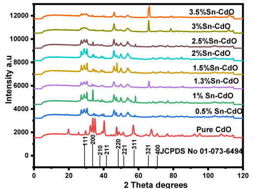
Figure 1. XRD spectra for the pure CdO and doped CdO with various concentration of tin prepared using wet chemical technique.
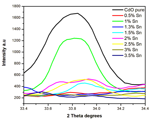
Figure 2. The XRD major intensity peaks for varying levels of tin for (111) plane synthesized using wet chemical process.
Debye Scherrer equation (1) was used to calculate the crystal size of nanoparticles .
D=βhklCosθ(1)
Where D is the crystal size, K is the constant equals 0.9, the wavelength of the radiation denoted byλ is 1.54960Å for copper Kα radiation, full width at half maximum (βhkl) and θis the peak position. A slight increase of Sn doping concentration (1%Sn) increases crystallite size of the nanoparticle from 20.07nm for pure CdO to 25.35nm tin doped, for 2.5%Sn the crystallite size increased to 24.45nm and further increase in doping (3.0%Sn) causes reduction of the crystallite size to 19.04nm. This could be attributed by a smaller amount of tin doping concentration allowing the crystals to coalesce hence enhancing crystallinity. Table 1 presents calculated crystallite sizes for plane (111) for pure and doped CdO.
Table 1. Tabulated crystallite sizes D (nm) for plane (111) for pure CdO and Sn doped CdO.

%Concentration of Sn

FWHM

β

Peak intensity

Crystallite size D (nm)

0

33.79

0.3957

0.006907

1651.99

20.07

0.5

33.80

0.1282

0.002237

297.19

61.98

1.0

33.81

0.3134

0.005470

1235.34

25.35

1.3

33.41

0.1491

0.002601

386.28

53.31

1.5

33.91

0.1666

0.002908

453.55

47.68

2.0

33.95

0.1204

0.002101

520.77

65.99

2.5

33.95

0.3249

0.005671

518.55

24.45

3.0

33.70

0.4167

0.007272

247.77

19.07

3.5

33.95

0.22168

0.003869

239.81

35.83

The lattice constant d was calculated using the Bragg’s equation (2)
=2dhklsinθ(2)
For Cadmium oxide face centered cubic structure, a=b=c therefore equation (3) was used to calculate lattice constant a
a=dhlkh2 +k2+l2(3)
The calculated values of lattice constant a, and d spacing presented in the table 2 shows that the lattice parameters deviate slightly from the standard values. According to JCPD file no 00-005-0640, plane (111) records d spacing of 0.2712 nm. The deviation is attributed to by the tin doped cadmium oxide trying to adopt the lattice constant for pure cadmium oxide during the reaction. Also, the presence of strain in the nanoparticles could contribute to the lattice parameters deviation from the standard values. The micro strain () values of the CdO: Snwere estimated using equation (4) .
ε=β4tanθ(4)
Where θ is the diffraction angle and β is the full width at half maximum. The length of the dislocation lines per unit volume that is dislocation density (δ) was calculated by means of Williamson and Smallman equation (5) .
δ =1D2(5)
Where D is the crystallite size obtained from the XRD results. Table 2 displays structural parameters for pure CdO and Sn doped CdO NPs prepared using wet chemical process. Generally, it was found that with increase in the doping concentration the strain and dislocation decrease. Although Sn⁴⁺ ions have a smaller ionic radius (0.69 Å) than Cd²⁺ ions (0.95 Å), allowing for substitution within the CdO lattice, the variation in crystallite size with increasing Sn concentration does not follow a strictly linear trend. At lower doping levels, the introduction of Sn can enhance crystallinity by improving lattice coherence, leading to larger crystallites as dopant atoms occupy substitutional sites with minimal distortion . From the calculated values of stress and dislocation density, it is clear that the CdO NPs faced some strain and defects. Therefore, as the doping concentration increases beyond an optimal point, excess Sn may have introduced localized strain, structural defects, or even form secondary phases (as observed in the XRD pattern), which can hinder grain growth and reduce the crystallite size. This competition between improved ordering at low concentrations and increased lattice distortion or defect accumulation at higher concentrations resulted in the observed non-monotonic trend in crystallite size. Similar behavior has been reported in other doped metal oxide systems, supporting this interpretation . Additionally, the variation in the crystallite sizes could be attributed to the particle agglomeration due to Ostwald ripening process where smaller particles combine to form larger particles .
Table 2. Structural parameters for pure CdO and Sn doped CdO.

Concentration of Sn used to dope CdO. (%)

d-spacing (nm)

Lattice parameter, a ()

Strain,E

Dislocation density, o

0

0.2650

4.589

0.3257

0.002483

0.5

0.2649

4.588

0.1055

0.0002603

1.0

0.2649

4.588

0.2578

0.001556

1.5

0.2641

4.4575

0.1366

0.0004399

2.0

0.2638

4.569

0.0985

0.0002296

2.5

0.2638

4.569

0.2661

0.001673

3.0

0.2657

4.602

0.3439

0.00275

3.5

0.2638

4.569

0.1814

0.000779

2.4.2. UV-Vis Analysis
The evolution of the optical properties of the as-prepared pure CdO and doped CdO NPs were monitored using UV-Vis absorption spectroscopy. The bandgap energy (Eg) of semi-conductor materials dispersed in liquid with known coefficient is mostly obtained using UV-Vis spectrometer. The nano powders of the samples were dispersed in a liquid of known absorption coefficient. The nanoparticles absorbed light at different wavelength depending on the doping concentration. Absorption edge for pure CdO was 298 nm and increased in the range of 300 nm to 340 nm for other samples when the dopant was introduced. The introduction of the dopant modifies the electronic properties of nanoparticles due to defects that result from stress, strain, interstitial and vacancies defects. The absorption wavelength of pure CdO is shorter compared to the standard wavelength and this could be due to the quantum confinement effect which arises as a result of formation of the CdO nanoparticles . This quantization causes an increase in band gap energy, causing the absorption edge to red shift in wavelength. Figure 4 shows the UV-Vis absorption spectra of pure CdO and CdO: Sn aliquot.
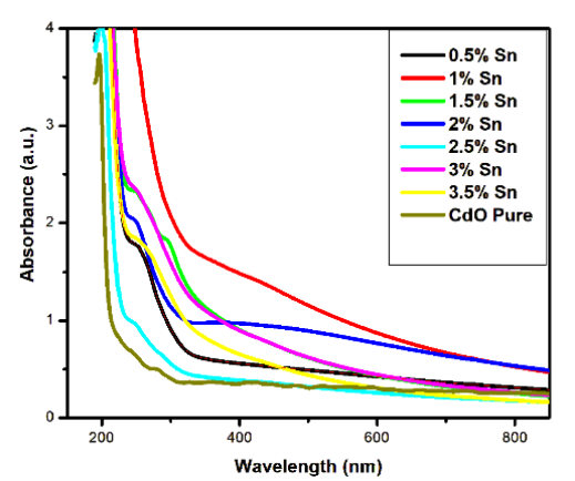
Figure 3. The evolution of absorbance spectra of different tin doping concentration.
Band Gap Analysis
The electronic structure of a material is defined by its band gap energy. Tauc relation equation (6) was used to predict the energy band gap of the as-obtained CdO and CdO: Sn NPs.
(αhv)γ=Ahv-AEg(6)
where αis the absorption coefficient, hv is the incident photon energy, γis allowed transition, A is a constant and Eg is the electronic band gap of the semiconductor material. When γ is 2 it is indirect and when ½ it is direct allowed transition from the valence band to transition. The values of the energy band gaps of the as-prepared NPs were approximated by drawing a tangent of (αhv)2 on Tauc’s plot and extrapolating to the (αhv)2 = 0 axis. Figure 4 shows the Tauc’s plot (a) and band gap energies for different doping concentration (b).
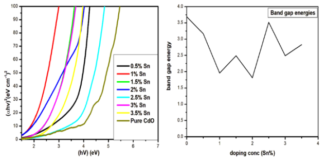
Figure 4. Tauc’s plot (a) and band gap energies of the NPs (b) for different Sn doping concentration.
From the Tauc’s plot the band gap energy for pure CdO NPs was 3.68 eV and for doped CdO NPs ranges from 1.81eV to 3.52eV depending on the dopant concentration. It is found that as the doping concentration of tin increases, the bandgap energies decrease. The bandgap energies for doped and undoped CdO nanoparticles differ from the standard values of the corresponding bulk material. The discrepancies could be attributed by the lattice strain and dislocations during the formation of the nanoparticles. Table 3 presents the summary of the bandgap energies (eV), absorption edge (nm) and the corresponding concentration of tin.
Table 3. Summarized table showing absorption edges and bandgap energies for different concentrations of tin doping.

Concentration of Sn used to dope CdO (%)

Absorption edge (nm)

Band gap energy (eV)

0

298

3.688

0.5

305

3.168

1.0

311

1.9566

1.5

315

2.4893

2.0

320

1.8120

2.5

295

3.5181

3.0

328

2.4893

3.5

337

2.8281

The increase in the UV region (298nm -337nm) with increasing tin doping concentration and reduction in band gap energy could be attributed to enhanced electronic transitions due to modification of the band structure . When Sn4+ ions are incorporated into CdO lattice, they substitute Cd2+ ions and introduce extra free electrons into the conduction band due to charge compensation . The increase in free carrier concentration leads to formation of defect states or shallow donor levels near conduction band from 3.688 eV to 1.812 eV. Also, variation in band gap energy observed with increasing Sn doping can be correlated with the structural changes identified in the XRD analysis. A decrease in crystallite size, as seen at higher doping concentrations, as determined by the Debye–Scherrer equation, suggests the presence of quantum confinement effects, which result in a widening of the band gap . Additionally, the increase in lattice strain and dislocation density, inferred from the broadening of XRD peaks, can also influence the electronic band structure by introducing localized states and altering the potential landscape within the crystal lattice . These strain-induced distortions can lead to changes in the band structure and contribute to the observed shifts in optical absorption edge. Thus, the nonlinear trend in band gap energy with Sn doping is consistent with the structural modifications revealed in the XRD analysis, where competing effects of improved crystallinity at low doping and increased defect density at higher doping levels play a significant role.
2.4.3. Photoluminescence (PL) Analysis
The photoluminescence properties of doped and undoped CdO nanoparticles were carried out at an ambient temperature and at an excitation wavelength of 320 nm, the photoluminescence properties of CdO were found to depend on the concentration of the dopant. Pure CdO was found to exhibit high luminance with an emission wavelength of 395nm compared to tin doped cadmium oxide which shows emission at wavelength in the range of 396nm to 400nm. Figure 5 shows photoluminescence emission spectra of CdO: Sn (a) and pure CdO (b).
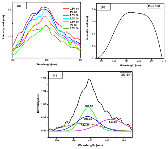
Figure 5. Photoluminescence emission spectra of tin doped cadmium oxide (CdO: Sn) (a), pure CdO (b) and deconvoluted graph of 3% Sn (c).
The intensity of emission peaks was found to decrease with increase in doping concentration. However, at a higher concentration of tin doping, photoluminescence quenching was observed. This could be due to surface recombination caused by Sn ions which creates surface states that act as traps for photogenerated electrons and holes, preventing them from participating in emission of light . This is also associated with the fact that highly doped nanoparticles excite electrons which can return to ground state without emitting photons. Table 4 shows a summary of tin doping concentration, emission wavelength and relative intensity for pure and doped CdO.
Table 4. Emission wavelengths, and relative intensity for pure and doped CdO NPs obtained fromPL spectra.

% Sn concentrations

Wavelength (nm)

Relative intensity (a. u.)

0

395

2.470

0.5

398

1.11

1.0

399

1.04

1.5

393

1.10

2.0

396

1.09

2.5

397

1.07

3.0

397

1.07

3.5

400

1.04

3. Conclusion
Undoped and tin doped cadmium oxide nanoparticles were successfully prepared using precipitation by reflux method. The study investigated structural and optical properties of pure CdO and CdO: Sn NPs with different concentration of tin (0.5, 1, 1.5, 2, 2.5, 3 and 3.5% to Cd). The XRD pattern displayed face centered cubic structure of cadmium oxide. Increase in the level of tin resulted in significant increase in grain size. Absorbance of the nanoparticles increased with increasing Sn dopant in the range of 298nm to 340nm and their corresponding band gap energy decreased with increase in the dopant (3.688 eV to 1.812 eV). The trend could be attributed to enhanced electronic transitions and increased free carrier absorption. PL properties showed a decrease in peak intensity of the nanoparticles when doping was increased and a shift in emission wavelength from 395nm for pure to 400nm in doping with 3.5% Sn. The synthesized nanoparticles possessed good structural and optical properties for possible solar cell applications.
Abbreviations

CdO

Cadmium Oxide

PL

Photoluminescence

XRD

X-ray Diffaction

UV-Vis

Ultra-violet and Visible

NPs

Nanoparticles

TCOs

Transparent Conducting Oxides

MPA

Mercapto-propionic Acid

JCPDS

Joint Committee on Powder Diffraction Standards

Eg

Band Gap

Acknowledgments
Thanks to the SG-NAPI ward supported by the German Ministry of Education and Research, BMBF through UNESCO-TWAS. Also wish to thank Murang’a University of Technology for providing us with synthesis and characterization equipment.
Author Contributions
Nancy Kiprotich: Conceptualization, Data curation, Formal Analysis, Funding acquisition, Investigation, Methodology, Supervision, Validation, Writing – original draft, Writing – review & editing
Peter Waithaka: Conceptualization, Data curation, Formal Analysis, Funding acquisition, Investigation, Methodology, Resources, Software, Supervision, Validation, Visualization, Writing – original draft, Writing – review & editing
Sharon Kiprotich: Conceptualization, Data curation, Formal Analysis, Funding acquisition, Investigation, Methodology, Project administration, Resources, Software, Supervision, Validation, Writing – original draft, Writing – review & editing
John Njagi: Conceptualization, Data curation, Formal Analysis, Investigation, Methodology, Supervision, Validation, Visualization, Writing – original draft, Writing – review & editing
Conflicts of Interest
The authors declare no conflicts of interest.
References
[1] S. Sharma, K. K. Jain, and A. Sharma, “Solar Cells: In Research and Applications—A Review,” Mater. Sci. Appl., vol. 06, no. 12, pp. 1145–1155, 2015,
[2] Ch. K. Lathaet al., “Effect of Capping Agent on the Morphology, Size and Optical Properties of In2O3 Nanoparticles,” Mater. Res., vol. 20, no. 1, pp. 256–263, Jan. 2017,
[3] U. D. Babar et al., “Study the photovoltaic performance of pure and Cd-doped ZnO nanoparticles prepared by reflux method,” Mater. Today Proc., vol. 43, pp. 2780–2785, Jan. 2021,
[4] N. M, M. M, P. V, J. Pawar, and R. Henry, “Synthesis And Characterization of Cadmium Oxide Nanoparticles for Antibacterial Activity,” in 2018 3rd International Conference on Communication and Electronics Systems (ICCES), Coimbatore, India: IEEE, Oct. 2018, pp. 195–197.
[5] E. M. Nasir, I. S. Naji, and M. F. A. Alias, “Characterization of Cadmium Tin Oxide Thin Films as a Window Layer for Solar Cell,” vol. 2, no. 9, 2013.
[6] A. Fall, J. Sackey, N. Mayedwa, and B. D. Ngom, “Investigation of structural and optical properties of CdO nanoparticles via peel of Citrus x sinensis,” Mater. Today Proc., vol. 36, pp. 298–302, 2021,
[7] T. Xaba, M. J. Moloto, M. A. Malik, and N. Moloto, “The Influence of Temperature on the Formation of Cubic Structured CdO Nanoparticles and Their Thin Films from Bis (2-hydroxy-1-naphthaldehydato) cadmium (II) Complex via Thermal Decomposition Technique,” J. Nanotechnol., vol. 2017, pp. 1–11, 2017,
[8] P. R. Sai and S. R. Marjorie, “Performance Analysis of the Conductivity of Pure Cadmium Oxide in Comparison with the Doped Cadmium Oxide using a Low Cost Technique,” in 2022 2nd International Conference on Technological Advancements in Computational Sciences (ICTACS), Tashkent, Uzbekistan: IEEE, Oct. 2022, pp. 86–90.
[9] A. S. Jasim, K. A. Aadim, and J. M. Hussein, “Preparation and fabrication of (Mg, Sn) doped CdO/PSi solar cell by laser induced plasma,” IOP Conf. Ser. Mater. Sci. Eng., vol. 928, no. 7, p. 072022, Nov. 2020,
[10] A. Kathalingam, K. Kesavan, A. U. H. S. Rana, J. Jeon, and H.-S. Kim, “Analysis of Sn Concentration Effect on Morphological, Optical, Electrical and Photonic Properties of Spray-Coated Sn-Doped CdO Thin Films,” Coatings, vol. 8, no. 5, p. 167, Apr. 2018,
[11] ZhenguoJi, Yueteng Yao, Junhua Xi, and Qiuhong Wu, “Deposition of transparent conducting CdO on flexible PET substrate,” in 2011 International Conference on Multimedia Technology, Hangzhou, China: IEEE, Jul. 2011, pp. 5799–5802.
[12] Department of Physical and Biological Sciences, Murang’a University of Technology, PO BOX 75, Murang’a 10200, Kenya and J. Jepngetich, “Effects of Ag Doping Concentrations on Structural and Optical Properties of Citrus Reticulata Capped ZnO Nanoparticles,” J. Nanosci. Res. Rep., pp. 1–7, Apr. 2025,
[13] N. M. Al-Hada, E. B. Saion, A. H. Shaari, M. A. Kamarudeen, M. H. Flaifel, and S. A. Gene, “Synthesis, Structural and Morphological Properties of Cadmium Oxide Nanoparticles Prepared by Thermal Treatment Method,” Adv. Mater. Res., vol. 1107, pp. 291–294, Jun. 2015,
[14] S. Kiprotich, F. B. Dejene, and M. O. Onani, “Effects of growth time on the material properties of CdTe/CdSe core/shell nanoparticles prepared by a facile wet chemical route,” Mater. Res. Express, vol. 9, no. 2, p. 025008, Feb. 2022,
[15] J. J. Sidor, “Quantitative Indicators of Microstructure and Texture Heterogeneity in Polycrystalline System,” Materials, vol. 17, no. 24, p. 6057, Dec. 2024,
[16] M. Othman, “Optical Characteristics of Cadmium Oxide and Magnesium Doped with Nanoclusters,” ECS J. Solid State Sci. Technol., vol. 11, no. 1, p. 013012, Jan. 2022,
[17] R. K. Leelavati and R. Kumar. "Structural and optical properties of CdO and Ni doped CdO nanomaterials." In AIP Conference Proceedings, vol. 2220, no. 1, p. 020140. AIP Publishing LLC, 2020.
[18] T. Prakash, E. Ranjith Kumar, K. Gnanamoorthi, Alaa M. Munshi, Samar J. Almehmadi, Gaber AM Mersal, and Nashwa M. El Metwaly. "Evaluation of phase, morphological, optical and electrical properties of microwave synthesized Sn doped CdO nanostructures." Solid State Communications 336 (2021): 114388.
[19] S. Kiprotich, B. F. Dejene, and M. O. Onani. "Effects of precursor pH on structural and optical properties of CdTe quantum dots by wet chemical route." J. Mat. Sci.: Mater. in Elec. Vol. 29, 16101-16110, July 2018.
[20] K. A. Aadim, B. M. Ahmed, and M. A. Khalaf, “Influence of Sn doping ratio on the structural and optical properties of CdO films prepared by laser induced plasma,” Iraqi J. Phys., vol. 18, no. 45, pp. 1–8, Jun. 2020,
[21] C. K. Gary Kwok, C. P. Liu, and K. M. Yu, “Sol-gel synthesis of highly transparent and conducting Cadmium Oxide,” in 2019 Compound Semiconductor Week (CSW), Nara, Japan: IEEE, May 2019, pp. 1–2.
[22] N. Rajkamal, K. Sambathkumar, M. Venkatachalapathy, and A. Bernick Raj. "Synthesis and Characterization of Some Metals (Sn, Ni, Zn, and Co) Doped with CdO Nanoparticles by Co-Precipitation Method for Super Capacitor Applications." Int. J. of Multidisciplinary Res. and Growth Eval. Vol. 4 no.3: 905–913.
[23] K. S. Mohammed, J. Mohammed M. Al-Zanganawee, and A. A. Kamil. "An investigation of (Co+ Zn) co-doping effect on certain physical features of nano-structured (CdO) thin films deposited by sol-gel spin coating technique." In AIP Conference Proceedings, vol. 2475, no. 1. AIP Publishing, 2023.
[24] N. Rathore, N. L. Panwar, F. Yettou, and A. Gama, “A comprehensive review of different types of solar photovoltaic cells and their applications,” Int. J. Ambient Energy, vol. 42, no. 10, pp. 1200–1217, Jul. 2021,
Cite This Article
  • APA Style

    Kiprotich, N., Waithaka, P., Kiprotich, S., Njagi, J. (2025). Effects of Tin Doping Concentration on the Structural and Optical Properties of Cadmium Oxide Nanoparticles. Advances in Materials, 14(2), 55-64. https://doi.org/10.11648/j.am.20251402.13

    Copy | Download

    ACS Style

    Kiprotich, N.; Waithaka, P.; Kiprotich, S.; Njagi, J. Effects of Tin Doping Concentration on the Structural and Optical Properties of Cadmium Oxide Nanoparticles. Adv. Mater. 2025, 14(2), 55-64. doi: 10.11648/j.am.20251402.13

    Copy | Download

    AMA Style

    Kiprotich N, Waithaka P, Kiprotich S, Njagi J. Effects of Tin Doping Concentration on the Structural and Optical Properties of Cadmium Oxide Nanoparticles. Adv Mater. 2025;14(2):55-64. doi: 10.11648/j.am.20251402.13

    Copy | Download

  • @article{10.11648/j.am.20251402.13,
      author = {Nancy Kiprotich and Peter Waithaka and Sharon Kiprotich and John Njagi},
      title = {Effects of Tin Doping Concentration on the Structural and Optical Properties of Cadmium Oxide Nanoparticles
    },
      journal = {Advances in Materials},
      volume = {14},
      number = {2},
      pages = {55-64},
      doi = {10.11648/j.am.20251402.13},
      url = {https://doi.org/10.11648/j.am.20251402.13},
      eprint = {https://article.sciencepublishinggroup.com/pdf/10.11648.j.am.20251402.13},
      abstract = {Wet chemical process was successfully used to synthesize tin doped and undoped cadmium oxide nanoparticles. Cadmium acetate, sodium hydroxide, mercaptopropionic acid and tin chloride were used as starting materials for synthesizing the nanoparticles. The reaction was carried out in a single three-necked flask under reflux at 80°C for 2 hours and the solution was allowed to cool to room temperature. The precipitate was washed, dried, annealed and grounded to obtain the powder for further analysis. The phase and structure of the nanoparticles was studied using the X-ray diffraction equipment. Debye Scherrer’s equation was used to calculate the crystallite sizes of the doped and undoped nanoparticles. The XRD pattern displayed face centered cubic structure of cadmium oxide. When CdO was doped with Sn the intensity peaks decreased from 1650 a. u for pure CdO to 1235 a. u at 1% Sn doped and at 3.5% Sn doped, the intensity peak was 239 a. u. Increase in the doping concentration resulted in significant increase in grain size. Optical properties investigated for different doping concentration of tin showed that all the samples exhibited the well-defined absorption bands in the range of 298 nm to 340 nm. The bandgap energy was found to be 3.69 eV for pure CdO and a realistic decrease when doped. The corresponding PL spectra with the excitation wavelength of 320 nm displayed a narrow emission at 429 nm. The obtained results displayed good material properties of the NPs suitable for possible solar cell applications.
    },
     year = {2025}
    }
    

    Copy | Download

  • TY  - JOUR
    T1  - Effects of Tin Doping Concentration on the Structural and Optical Properties of Cadmium Oxide Nanoparticles
    
    AU  - Nancy Kiprotich
    AU  - Peter Waithaka
    AU  - Sharon Kiprotich
    AU  - John Njagi
    Y1  - 2025/06/30
    PY  - 2025
    N1  - https://doi.org/10.11648/j.am.20251402.13
    DO  - 10.11648/j.am.20251402.13
    T2  - Advances in Materials
    JF  - Advances in Materials
    JO  - Advances in Materials
    SP  - 55
    EP  - 64
    PB  - Science Publishing Group
    SN  - 2327-252X
    UR  - https://doi.org/10.11648/j.am.20251402.13
    AB  - Wet chemical process was successfully used to synthesize tin doped and undoped cadmium oxide nanoparticles. Cadmium acetate, sodium hydroxide, mercaptopropionic acid and tin chloride were used as starting materials for synthesizing the nanoparticles. The reaction was carried out in a single three-necked flask under reflux at 80°C for 2 hours and the solution was allowed to cool to room temperature. The precipitate was washed, dried, annealed and grounded to obtain the powder for further analysis. The phase and structure of the nanoparticles was studied using the X-ray diffraction equipment. Debye Scherrer’s equation was used to calculate the crystallite sizes of the doped and undoped nanoparticles. The XRD pattern displayed face centered cubic structure of cadmium oxide. When CdO was doped with Sn the intensity peaks decreased from 1650 a. u for pure CdO to 1235 a. u at 1% Sn doped and at 3.5% Sn doped, the intensity peak was 239 a. u. Increase in the doping concentration resulted in significant increase in grain size. Optical properties investigated for different doping concentration of tin showed that all the samples exhibited the well-defined absorption bands in the range of 298 nm to 340 nm. The bandgap energy was found to be 3.69 eV for pure CdO and a realistic decrease when doped. The corresponding PL spectra with the excitation wavelength of 320 nm displayed a narrow emission at 429 nm. The obtained results displayed good material properties of the NPs suitable for possible solar cell applications.
    
    VL  - 14
    IS  - 2
    ER  - 

    Copy | Download

Author Information