Research Article | | Peer-Reviewed

Effects of Electrolyte Concentrations and Annealing on Some Surface Characteristics of Optimised Electrochemical Deposited Tin-(II)-Sulphide (SnS) Thin Films

Received: 10 March 2026     Accepted: 23 March 2026     Published: 7 April 2026
Views:       Downloads:
Abstract

This study set out to address the issue of having cost effective and environmental benign material as absorber layer of thin film solar cells. Thus, the study reported the results of some surface characterization of optimized two-electrode electrochemical deposited Tin-(II)-Sulphide (SnS) thin films. The films were prepared from analytical grade chemical salts of tin (II) tetraoxosulphate (VI) [SnSO4] and sodium thiosulphate pentahydrate [Na2S2O3.5H2O]. They were deposited on ITO coated glass. Some samples were annealed in a Carbonite cylindrical tube furnace at 350°C for one (1) hour under an inert argon atmosphere. The samples (as-deposited and annealed) were then characterized using X-Ray Diffraction (XRD) for structural analysis while surface morphology was determined using Scanning Electron Microscopy (SEM). The data obtained were analyzed using Origin version 2018 to obtain diffraction patterns and three dimension (3D) interactive surface plots of the micrographs were performed using ImageJ software. The results reveal that two-electrode electrochemical deposition technique is a suitable technique for depositing optimum SnS for photon absorption and that, both electrolyte concentration and annealing have positive influence on the structure and morphology of the film. The film intensity, crystallinity and phase purification increase with electrolyte concentration while annealing enhance the grain size and surface uniformity of the films. Thus, it was recommended that, the SnS thin films for photovoltaic application should be prepared from optimum electrolyte concentration using two-electrode electrochemical deposition method and annealed at 350°C in inert environment for the fabrication of thin film solar cells.

Published in Advances in Materials (Volume 15, Issue 2)
DOI 10.11648/j.am.20261502.11
Page(s) 27-36
Creative Commons

This is an Open Access article, distributed under the terms of the Creative Commons Attribution 4.0 International License (http://creativecommons.org/licenses/by/4.0/), which permits unrestricted use, distribution and reproduction in any medium or format, provided the original work is properly cited.

Copyright

Copyright © The Author(s), 2026. Published by Science Publishing Group

Keywords

Electrolyte, Annealing, Tin-(II)-Sulphide (SnS), Electrochemical Deposition, Surface Characteristics, Thin Films

1. Introduction
Global demand for electricity is increasingly rising due to population growth, technological advancements and improved standard of living which revolve around heavy usage of electricity . At present, large percentage of electricity in circulation is generated from fossil fuels such as coal, petroleum and natural gas. These sources of electricity pose environmental challenges in terms of emission of greenhouse gases which causes global warming and environmental degradations . This is couple with the fact that fossil fuels are non-renewable natural sources of energy and are depletable . Thus, there is a need for alternative source of generating electricity. There are several renewable alternatives source of generating electricity such as Geothermal, Wind, Hydro and Solar (Photovoltaics) cells. However, Photovoltaics stand out unique especially for Nigeria where the solar radiation is available all the year round. Photovoltaic cells are electronic devices that trap sunlight radiation for conversion into electrical energy by photovoltaic effects.
Solar cells manufactured from wafers of crystalline or polycrystalline silicon are today the dominant technology in the commercial market but are rather costly. Thin film solar cells that use thin layers of photovoltaic materials, which convert sunlight into electricity have now emerged as a solution. New types of thin-film solar cells made from non-toxic and abundant materials with adequate physical properties such as close optimum band-gap energy, large absorption co-efficient and p-type conductivity are needed to replace Cu(In, Ga)Se2 and CdTe absorber technologies whose elemental components are scarce and toxic . Tin (II) sulphide (SnS) is a promising material for thin film solar cells due to its more favourable optoelectronic characteristics such as suitable bandgap energy, high absorption coefficient and non-toxicity. However, the efficiency of SnS-based solar cells is still limited by the quality of the SnS thin films obtained from deposition techniques . Electrochemical deposition (ECD) method is a widely adopted technique which uses electrolytic set up for depositing light-absorbing thin films used in solar cells. ECD involves a simple, inexpensive and environmentally compatible process that produce high quality films . However, careful optimisation is required to produce SnS thin films of desired properties that will yield low cost of high efficiency solar cells. Therefore, this study reports the effect of electrolyte concentration and annealing on the structural and morphological characteristics of two-electrodes electrochemical deposited SnS thin films that could lead to optimum photon absorption.
2. Materials and Method
Analytical grade chemical salts -tin (II) tetraoxosulphate (VI) [SnSO4] and sodium thiosulphate pentahydrate [Na2S2O3.5H2O] (Sigma-Aldrich), reagents- isopropanol, acetone, tetraoxosulphate (VI) acid and distilled water from the Chemistry laboratory I, Department of Chemistry, Federal University of Education, Kontagora, Niger State, Nigeria were used as received throughout the experiments. Glass wares and Indium Tin Oxide (ITO) coated glasses were ultrasonically washed and dried. All experiments were carried out at room temperature.
The precursors, solutions of 0.01 M and 0.05 M tin (II) tetraoxosulphate (VI) [SnSO4] and 0.05 M and 0.1 M sodium thiosulphate pentahydrate [Na2S2O3.5H2O] were prepared. The detail is as in Table 1. A two-electrode electrochemical cell set up as shown in Figure 1 consisting of working electrode (ITO coated glass) and counter electrode (graphite plate) at about 32.5 mm distance was used. The electrodes were immersed in an electrolytic bath of 25 mL SnSO4, 25 mL Na2S2O3.5H2O as the sources of Sn2+ and S2- ions respectively and 2 drops of 0.05 M H2SO4 solutions as pH adjuster. At pH 2.5 and applied voltage of 1.5 V, tin (II) sulphide [SnS] thin films samples A and B were deposited on the working electrode from the respective bath mixtures of 0.01 M SnSO4 and 0.05 M Na2S2O3.5H2O and 0.05 M SnSO4 and 0.1 M Na2S2O3.5H2O at 1080/18 and 1320/22 seconds/minutes deposition periods respectively as detailed in Table 1.
Table 1. Detail Deposition Parameters.

Samples/Materials

Sample A

Sample B

SnSO4

0.537 g / 250 ml

2.685 g / 250ml

Molarity

0.01 M

0.05 M

Na2S2O3.5H2O

3.102 g / 250 ml

6.204 g / 250 ml

Molarity

0.05 M

0.1 M

Applied Voltage

1.5 A

1.5 A

Electrolyte bath pH

2.5

2.5

Deposition Period

1080/18 Seconds/Minutes

1320/22 Seconds/Minutes

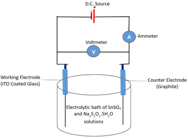
Figure 1. Schematic Diagram of Two Electrodes Electrochemical Set Up Employed.
The electrodeposited thin films were carefully removed, rinsed with distilled water and placed in separate well labelled sample holders for annealing and characterization.
Samples were annealed in a Carbonite cylindrical tube furnace at 350°C for 1 hour under an inert argon atmosphere to prevent oxidation. One of the rationales for annealing was to enhance the crystallinity and facilitate phase transformation of the as-deposited material, which is crucial in optimizing material performance in photovoltaic devices. The furnace was purged with high-purity argon gas (99.999%) for 15 minutes pre-heating and maintained with a continuous argon flow throughout the annealing process. The heating rate was 5°C/min, and samples were allowed to cool naturally to room temperature under argon gas.
The samples [as-deposited (unannealed) and annealed] were then characterized using X-Ray Diffraction (XRD) for structural analysis and surface morphology was determined using Scanning Electron Microscopy (SEM). Powered X-ray diffraction (XRD) analysis was employed to analyze the sample diffraction spectra pattern using a Bruker D2 Phaser diffractometer with Cu Kα radiation (λ = 1.5406 Å) operated at 30 kV and 10 mA. Samples were loaded unto the Diffractometer stage and scanned through a 2θ range of 10°–90° with a step size of 0.02° and a scan speed of 1°/min. Diffraction data obtained from the samples were acquired using the DIFFRAC. EVA software suite. The exported ASCII data were further processed with Origin version 2018 to obtain diffraction patterns.
The surface morphology of samples was examined using a Tescan Vega thermionic Scanning Electron Microscope (SEM). The SEM was operated at an accelerating voltage of 15 kV. Samples were mounted on aluminum stubs using conductive carbon tape and sputter-coated with a thin layer of gold to enhance surface conductivity. Micrographs were captured in Secondary Electron (SE) mode. Average particle size and 3D interactive surface plots of the micrographs were performed using ImageJ software.
3. Results and Discussion
The results obtained from the Structural and Morphological characterization of the as-deposited (unannealed) and annealed samples and their discussions were presented as follows:
3.1. Structural Characterization of As-deposited Samples
The peaks obtained from the XRD data were matched using the origin software 2018 with the Gaussian mode. The result of the peak matching is shown in Figure 2. The figure presents flat random fluctuations near zero with very few outliers and the normally distributed curve in the residual plots, these are indicative of a good fit between the Gaussian model and the experimental data obtained from the samples. Hence data was used for phase identification.
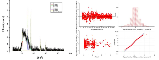
Figure 2. Peak matching and Residual plots.
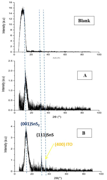
Figure 3. XRD Spectra for the blank and as-deposited thin film samples A and B.
X-ray diffraction patterns of the blank, as-deposited (un-annealed) samples of the two concentrations of electrochemically deposited Tin-(II)-Sulphide on ITO are presented in Figure 3. In Figure 3 the blank thin film holder had one near zero broad peak while the samples A and B produced peak at 15° (001) SnS2 and another peak at 31° (111) SnS in sample A. A third clearer peak was observed in sample B at 35° (400) ITO. These peaks obtained in A and B samples represent a polycrystalline hexagonal and orthorhombic phases SnS2 and SnS respectively. This agrees with data reported in previous studies and the Inorganic Crystal Structure Database (ICSD) The SnS phase grew along the (111) plane, while that of SnS2 phase was evident along the (001) plane. It can also be observed that the peak intensity in sample A is lower than the corresponding peaks in sample B. This could relate to the effect of the concentration on the samples. An electrodeposition study also reported that as SnSO₄ concentration increases, the intensity of pure SnS peaks increases indicating stronger crystallinity and phase purity with higher tin precursor concentration . This is in tandem with the results obtained in this study where the higher concentration of SnSO₄ in B produced peaks with higher intensity as depicted in Figure 3.
3.2. Structural Characterization of Annealed Samples
Annealed samples of Tin sulphide (SnS) were analysed using XRD. Fine peaks of the samples were observed after annealing and hence, peak matching was done with the Origin Lab 2018 software. The XRD patterns are shown in Figure 4.
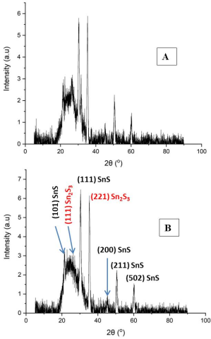
Figure 4. XRD Spectra for the annealed samples A and B at 350°C.
Samples A and B after annealing at 350 oC produced similar spectra with same number of peaks as depicted in Figure 4. The peaks were more enhanced and better defined compared to the un-annealed samples Figure 3. Sharper peaks produced could infer higher crystallinity in the materials. Phase identification was performed by matching the peaks and comparing the results with ICSD and other publication .
The annealed samples A and B showed reflections from the (111), and (221) planes of orthorhombic Sn2S3 phase and the rest of the planes maintained the (111). However, there was a significant change in the phase composition with the growth of lines (101), (200), (211), and (502) planes of the orthorhombic SnS phase. The SnS2 (001) line disappeared affirming a thermally induced phase transition from the hexagonal SnS2 to the Orthorhombic Sn2S3 and SnS phases. Generally, Sn₂S₃ tends to form around 300–400°C .
It can also be observed that though the peaks in samples A and B are at the same positions, the intensity of the peaks are slightly higher compared to the intensities as previously observed in the un-annealed samples. It has been observed in previous studies that the concentration of SnSO₄ (tin sulphate) in the bath does affect the intensity of XRD peaks, which is directly related to the crystallinity and growth mode of the deposited film. Recent studies on SnS electro-deposition using 0.1 M SnSO₄ (with varying Na₂SO₄ concentrations) reports that XRD peak intensities and preferred orientation of SnS changed notably with precursor concentrations; and that higher concentration of SnSO4 could be responsible for these increased peak intensities.
3.3. Surface Morphological Study of the Un-annealed and Annealed Samples
The surface morphology of the un-annealed and the annealed samples were scanned using the Tescan Vega SEM for samples A and B are as shown in Figures 5 and 6.
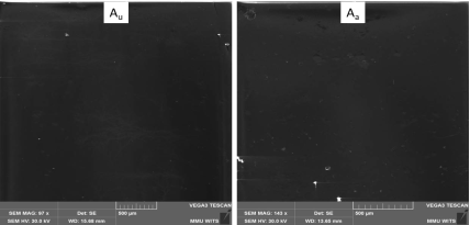
Figure 5. SEM 500 µm Micrographs for Sample A: Un-annealed (Au) and the Annealed (Aa).
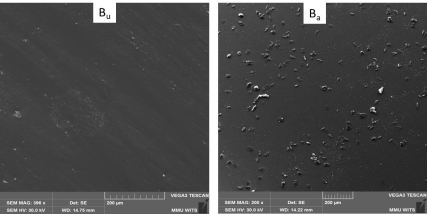
Figure 6. SEM 200 µm Micrographs for Sample B: Un-annealed (Bu) and the Annealed (Ba).
In Figure 5, the as-deposited (un-annealed) sample (Au) exhibited smaller particle sizes compared to the annealed sample (Aa), with surface voids appearing more prominent in Aa than in Au. This trend is more pronounced in Figure 6, where in the annealed sample (Ba), the particles are noticeably larger and better defined than (Bu), indicating grain growth resulting from thermal annealing and recrystallization due to grain boundary migration during heat treatment. This is consistent with the study conducted by .
3.4. Particle Size Distribution of the SEM Micrographs
The surface morphology of tin sulphide (SnS) thin films was analyzed by measuring the particle size distribution from SEM micrographs of two samples (A and B). Each sample was studied in both un-annealed and annealed conditions to assess the effect of thermal treatment at 350°C on average particle size. The results are shown in Table 2.
Table 2. Average Particle Size Before and After Annealing.

Sample

Condition

Average Particle Size (µm)

SD

N

Au

Un-annealed

95.2

260.4

59

Aa

Annealed

78.7

149.9

41

Bu

Un-annealed

108.9

6018.6

16066

Ba

Annealed

34.4

96

2040

Sample Au had an average particle size of 95.2 µm with a standard deviation of 260.4 µm, showing a wide and heterogeneous grain size distribution. After annealing at 350°C, the average particle size of Aa decreased slightly to 78.7 µm with a corresponding reduction in standard deviation to 149.9 µm. This lowering of size distribution reflects that annealing led to surface reorganization and some refinement of the grains, this could have been possibly by elimination of microstructural defects and coalescence of loosely connected grains. The results indicate a minimal improvement in surface uniformity and morphological compactness after thermal treatment.
In sample B however, the un-annealed sample (Bu), had a higher average particle size of 108.9 µm and a very high standard deviation of 6018.6 µm, which could be a reflection of heavy particle agglomeration and highly irregular growth in as-deposited state. Post-annealing, the average particle size of sample Ba was reduced heavily to 34.4 µm, and the standard deviation dropped substantially to 96.0 µm, this could depict a high homogenization of the surface morphology. The clear difference indicates that thermal treatment of the samples at 350°C not only promoted grain migration but also facilitated fragmenting of large agglomerates, resulting in a more homogeneous and finer microfilm structure. This finding is in tandem with the findings of .
The difference in responses of Sample A and Sample B to thermal annealing could be due to the varying precursor concentrations, which could have influenced initial nucleation and growth. In general, the results indicate that annealing at 350°C significantly influenced grain refinement and morphological uniformity in SnS thin film. The extent of such an influence is largely governed by the deposition conditions, namely concentration, which dictates the type and scale of microstructural transformation upon post-deposition heat treatment.
3.5. Surface Uniformity of the SEM Micrographs
Surface uniformity using 3D interactive surface plot was employed in analysis of the SEM micrographs. The results are shown in Figures 7 and 8.
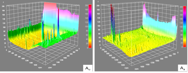
Figure 7. Three-Dimensional (3D) Surface Plots of Un-annealed and the Annealed Samples A.
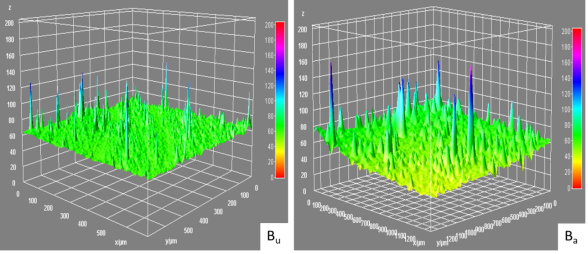
Figure 8. Three-Dimensional (3D) Surface Plots of Un-annealed and the Annealed Samples B.
The 3D interactive surface plots of the Tin-II-sulphide (SnS) thin film samples illustrate clear morphological developments caused by both the concentration and thermal annealing at 350°C.
The un-annealed Sample Au exhibited a coarse and very jaggy surface, indicative of low surface flatness and underdeveloped grain structures. Following annealing at 350°C, the surface was less jaggy and much smoother with the growth of finer and more evenly distributed island-like features. This morphological improvement of the surface is indicative of enhanced grain growth and recrystallization due to higher thermally activated surface diffusion which is in agreement with the findings of .
Un-annealed Sample Bu exhibited a rough and jagged surface, similar to that of Sample Au but with a more developed grains structure. This is likely due to the higher material load as a result of higher concentration of electrolyte bath. After annealing, the surface became less rough but unlike that of Sample Aa, it showed larger and more discrete islands. The formation of the larger islands could be indicative of the higher concentration, which promotes thicker film deposition and coalescence upon annealing as earlier reported by .
Surface morphology plays a crucial role in determining optoelectronic performance of absorber layers for photovoltaic devices . Thus, the more uniform the surface of thin films is, the better is its performance as absorber material in solar cells. This implies that annealing of thin films enhances their photon absorption. Thus, the annealed Sample Aa with less rough and more even surface and smaller islands could be inferred to exhibit enhanced light absorption, reduced surface recombination sites, and enhanced charge carrier mobility, all of which are beneficial for efficiency of any photovoltaic device made from this material. In contrast, the bigger islands in annealed Sample Ba presumably increasing light scattering thus, reduced photon absorption and may also introduce non-uniform electric fields thus increases local recombination centers, which will limit charge transport.
4. Conclusion and Recommendation
The study concludes that, two electrodes electrochemical deposition is a suitable deposition technique for depositing SnS thin films suitable as absorber layer in SnS based thin film solar cells. That, both electrolyte concentration and annealing influence the crystallization and surface uniformity of two-electrodes electrochemical deposited Tin-(II)-sulphide (SnS) thin films. That the sample A deposited from 0.01 M of SnSO4 and 0.05 M of Na2S2O3.5H2O and annealed at 350 oC yield the SnS thin films that could give optimum photon absorption.
The study therefore recommends that, two electrodes electrochemical deposited SnS thin films deposited using 0.01 M of SnSO4 and 0.05 M of Na2S2O3.5H2O and annealed at 350 oC should be employed in the fabrication of SnS based thin film solar cells. Thus, the deposition of the absorber layer Tin-(II)-Sulphide (SnS) based thin film solar cells should be prepared via two-electrode electrochemical deposition technique that utilizes less quantity of materials and introduce far less waste to the environment to attain cheaper and environmental benign solar cells.
Abbreviations

3D

Three Dimension

Ecd

Electro Chemical Deposition

ITO

Indium Tin Oxide

SEM

Scanning Electron Microscope

XRD

X-Ray Diffractometer

Acknowledgments
The research team were grateful to Nigeria Tertiary Education Trust Fund (tetfund) for sponsorship of the research through the Institutional Based Research (IBR) 2023/2024 research grant and to the University management for recommending this research for sponsorship. The trio of Dr. N. C. Gatsi, Dr. Geoffrey Nwendwa and Dr. Nyiku Mahonisi of School of Physics, University of Witswatersrand, South Africa for their assisting both material and technical during the annealing stage of the sample.
Author Contributions
Akangbe Ramoni Lasisi: Conceptualization, Data curation, Formal Analysis, Funding acquisition, Investigation, Methodology, Project administration, Resources, Supervision, Writing – original draft, Writing – review & editing
Samuel Tergunwa Temaugee: Data curation, Formal Analysis, Funding acquisition, Investigation, Methodology, Resources, Writing – original draft, Writing – review & editing
Abubakar Idris Dangana: Data curation, Funding acquisition, Investigation, Methodology, Writing – original draft
Alimi Taofeek: Data curation, Funding acquisition, Investigation, Methodology, Writing – original draft, Writing – review & editing
Umar Abubakar: Data curation, Funding acquisition, Investigation, Methodology, Writing –original draft
Conflicts of Interest
The authors declare that there are no conflicts of interest.
References
[1] Ajibade, A. A. (2019). National Strategies to Promote Renewable Energy Development: Whither Nigeria? Afe Babalola University Journal of Sustainable Development, Law & Policy, 10, 1, 74 -103.
[2] Bagher, A. M., Vahid, M. M. A. and Mohsen, M. (2015). Types of Solar Cells and Application. American Journal of Optics and Photonics. 3, 5, 94-113.
[3] Boubakri, A., Koumya, Y., Rajira, A., Almaggoussi, A., Abounadi, A., & Achargui, N. (2023). Triethanolamine concentration effect on electrodeposited SnS thin films properties. Journal of Solid State Electrochemistry, 27, 5, 1061–1074.
[4] Bronusiene, A., Barauskiene, I., Popov, A., Zsiros, B., Farkas, A., Plšek, J., & Ancutiene, I. (2024). The Impact of Thermal Treatment on the Structural, Optical and Electrochemical Characteristics of Tin Sulfide Films. Coatings, 14, 10.
[5] Cifuentes, C., Botero, M., Romero, E., Calderón, C., & Gordillo, G. (2006). Optical and structural studies on SnS films grown by co-evaporation. Brazilian Journal of Physics, 36, 1046–1049.
[6] Dekhil, D., Guessas, H., Nouri, A., & Ullah, S. (2023). Annealing effect on the photocurrent response of SnS thin films prepared by the chemical spray pyrolysis method. Chalcogenide Letters, 20, 8, 549–558.
[7] Ganchev, M., Spasova, S., Raadik, T., Mere, A., Altosaar, M. and Mellikov, E. (2023). Rapid Thermal Processing of Kesterite Thin Films. Coatings, 13, 1-14.
[8] Gardinier, C. F., & Chang, L. L. Y. (1978). Phase relationships in the systems Mo-Sn2S, W2Sn2S and Mo2W2S. Journal of the Less Common Metals, 61, 2, 221–229.
[9] Gedi, S., Minnam Reddy, V. R., Alhammadi, S., Park, H., Jang, C., Park, C., & Kim, W. K. (2021). Synthesis and Characterization of π-SnS Nanoparticles and Corresponding Thin Films. Nanomaterials, 11, 3, 767.
[10] Guo, W. (2016). The problem of the overuse of the fossil fuel to produce electricity. School of North China Electric Power University, Bao Ding 5th International Conference on Advanced Materials and Computer Science (ICAMCS 2016), 788-790.
[11] Hassan, T. A. (2016). Thermal Annealing Effects on Characterization of Tin Sulfide Thin Films. 2, 6.
[12] Hegde, S. S., Kunjomana, A. G., Murahari, P., Prasad, B. K., & Ramesh, K. (2018). Vacuum annealed tin sulfide (SnS) thin films for solar cell applications. Surfaces and Interfaces, 10, 78–84.
[13] Jin, L., Duan, K. and Tang, X. (2018). What Is the Relationship between Technological Innovation and Energy Consumption? Empirical Analysis Based on Provincial Panel Data from China. Sustainability, 10, 145.
[14] Kehinde, O., Babaremu, K. O., Akpanyung, K. V., Remilekun, E., Oyedele, S. T. and Oluwafemi, J. (2018). Renewable Energy in Nigeria- A Review. International Journal of Mechanical Engineering and Technology, 9, 10, 1085–1094.
[15] Lasisi, A. R., Babalola O. A., Taleatu, B. A., Alabi, A. B. & Akomolafe, T. (2016) Fabrication and Characterization of Tin Sulphide (SnS) Based Thin Film Solar Cells. Asian Journal of Science and Technology, 7, 11, 3887 - 3890.
[16] Lovchinov, K., Gergova, R., Alexieva, G. (2022). Structural, Morphological and Optical Properties of Nanostructured ZrO2 Films Obtained by an Electrochemical Process at Different Deposition Temperatures. Coatings, 12, 972.
[17] Ma, S., Li, S., Luo, Q., Yu, Z. and Wang, Y. (2024). Revisiting the relationships between energy consumption, economic development and urban size: A global perspective using remote sensing data. Heliyon, 10, 24, 1-15.
[18] Mare, S. D., Menossi, D., Salavei, A., Artegiani, E., Piccinelli, F., Kumar, A., Mariotto, G. and Romeo, A. (2017). SnS thin film solar cells: Perspectives and limitations. Coatings, 7, 2, 34-46.
[19] Mo, Z., Chu, X., Gao, P., Yang, D., Cui, H., Fang, Y., Li, H., Yin, X., & Zhao, Z. (2021). Effect of Continuous Annealing Temperature on the Microstructure, Mechanical Properties and Texture of Annealed Drawn and Ironed Plate. Crystals, 11, 12. Article 12.
[20] Nogami, T., Suzuki, I., Motai, D., Tanimura, H., Ichitsubo, T., & Omata, T. (2025). Non-stoichiometry in SnS: How it affects thin-film morphology and electrical properties. APL Materials, 13, 3, 031115.
[21] Olujobi, O. J. and Olujobi, T. O. (2020). Nigeria: Advancing the Cause of Renewable Energy in Nigeria’s Power Sector Through its Legal Framework. Environmental Policy and Law 50, 433–444.
[22] Reghima, M., Akkari, A., Guasch, C., & Turki-Kamoun, N. (2014). Structure, Surface Morphology, and Optical and Electronic Properties of Annealed SnS Thin Films Obtained by CBD. Journal of Electronic Materials, 43, 9, 3138–3144.
[23] Voznyi, A., Kosyak, V., Grase, L., Vecstaudža, J., Onufrijevs, P., Yeromenko, Yu., Medvid’, A., & Opanasyuk, A. (2018). Formation of SnS phase obtained by thermal vacuum annealing of SnS2 thin films and its application in solar cells. Materials Science in Semiconductor Processing, 79, 32–39.
[24] Wu, K.-J., Tse, E. C. M., Shang, C., & Guo, Z. (2022). Nucleation and growth in solution synthesis of nanostructures – From fundamentals to advanced applications. Progress in Materials Science, 123, 100821.
[25] Zaki, S. A., Abd-Elrahman, M. I., Abu-Sehly, A. A., Shaalan, N. M., & Hafiz, M. M. (2018). Thermal annealing of SnS thin film induced mixed tin sulfide oxides-Sn2S3 for gas sensing: Optical and electrical properties. Materials Science in Semiconductor Processing, 75, 214–220.
Cite This Article
  • APA Style

    Lasisi, A. R., Temaugee, S. T., Dangana, A. I., Taofeek, A., Abubakar, U. (2026). Effects of Electrolyte Concentrations and Annealing on Some Surface Characteristics of Optimised Electrochemical Deposited Tin-(II)-Sulphide (SnS) Thin Films. Advances in Materials, 15(2), 27-36. https://doi.org/10.11648/j.am.20261502.11

    Copy | Download

    ACS Style

    Lasisi, A. R.; Temaugee, S. T.; Dangana, A. I.; Taofeek, A.; Abubakar, U. Effects of Electrolyte Concentrations and Annealing on Some Surface Characteristics of Optimised Electrochemical Deposited Tin-(II)-Sulphide (SnS) Thin Films. Adv. Mater. 2026, 15(2), 27-36. doi: 10.11648/j.am.20261502.11

    Copy | Download

    AMA Style

    Lasisi AR, Temaugee ST, Dangana AI, Taofeek A, Abubakar U. Effects of Electrolyte Concentrations and Annealing on Some Surface Characteristics of Optimised Electrochemical Deposited Tin-(II)-Sulphide (SnS) Thin Films. Adv Mater. 2026;15(2):27-36. doi: 10.11648/j.am.20261502.11

    Copy | Download

  • @article{10.11648/j.am.20261502.11,
      author = {Akangbe Ramoni Lasisi and Samuel Tergunwa Temaugee and Abubakar Idris Dangana and Alimi Taofeek and Umar Abubakar},
      title = {Effects of Electrolyte Concentrations and Annealing on Some Surface Characteristics of Optimised Electrochemical Deposited Tin-(II)-Sulphide (SnS) Thin Films},
      journal = {Advances in Materials},
      volume = {15},
      number = {2},
      pages = {27-36},
      doi = {10.11648/j.am.20261502.11},
      url = {https://doi.org/10.11648/j.am.20261502.11},
      eprint = {https://article.sciencepublishinggroup.com/pdf/10.11648.j.am.20261502.11},
      abstract = {This study set out to address the issue of having cost effective and environmental benign material as absorber layer of thin film solar cells. Thus, the study reported the results of some surface characterization of optimized two-electrode electrochemical deposited Tin-(II)-Sulphide (SnS) thin films. The films were prepared from analytical grade chemical salts of tin (II) tetraoxosulphate (VI) [SnSO4] and sodium thiosulphate pentahydrate [Na2S2O3.5H2O]. They were deposited on ITO coated glass. Some samples were annealed in a Carbonite cylindrical tube furnace at 350°C for one (1) hour under an inert argon atmosphere. The samples (as-deposited and annealed) were then characterized using X-Ray Diffraction (XRD) for structural analysis while surface morphology was determined using Scanning Electron Microscopy (SEM). The data obtained were analyzed using Origin version 2018 to obtain diffraction patterns and three dimension (3D) interactive surface plots of the micrographs were performed using ImageJ software. The results reveal that two-electrode electrochemical deposition technique is a suitable technique for depositing optimum SnS for photon absorption and that, both electrolyte concentration and annealing have positive influence on the structure and morphology of the film. The film intensity, crystallinity and phase purification increase with electrolyte concentration while annealing enhance the grain size and surface uniformity of the films. Thus, it was recommended that, the SnS thin films for photovoltaic application should be prepared from optimum electrolyte concentration using two-electrode electrochemical deposition method and annealed at 350°C in inert environment for the fabrication of thin film solar cells.},
     year = {2026}
    }
    

    Copy | Download

  • TY  - JOUR
    T1  - Effects of Electrolyte Concentrations and Annealing on Some Surface Characteristics of Optimised Electrochemical Deposited Tin-(II)-Sulphide (SnS) Thin Films
    AU  - Akangbe Ramoni Lasisi
    AU  - Samuel Tergunwa Temaugee
    AU  - Abubakar Idris Dangana
    AU  - Alimi Taofeek
    AU  - Umar Abubakar
    Y1  - 2026/04/07
    PY  - 2026
    N1  - https://doi.org/10.11648/j.am.20261502.11
    DO  - 10.11648/j.am.20261502.11
    T2  - Advances in Materials
    JF  - Advances in Materials
    JO  - Advances in Materials
    SP  - 27
    EP  - 36
    PB  - Science Publishing Group
    SN  - 2327-252X
    UR  - https://doi.org/10.11648/j.am.20261502.11
    AB  - This study set out to address the issue of having cost effective and environmental benign material as absorber layer of thin film solar cells. Thus, the study reported the results of some surface characterization of optimized two-electrode electrochemical deposited Tin-(II)-Sulphide (SnS) thin films. The films were prepared from analytical grade chemical salts of tin (II) tetraoxosulphate (VI) [SnSO4] and sodium thiosulphate pentahydrate [Na2S2O3.5H2O]. They were deposited on ITO coated glass. Some samples were annealed in a Carbonite cylindrical tube furnace at 350°C for one (1) hour under an inert argon atmosphere. The samples (as-deposited and annealed) were then characterized using X-Ray Diffraction (XRD) for structural analysis while surface morphology was determined using Scanning Electron Microscopy (SEM). The data obtained were analyzed using Origin version 2018 to obtain diffraction patterns and three dimension (3D) interactive surface plots of the micrographs were performed using ImageJ software. The results reveal that two-electrode electrochemical deposition technique is a suitable technique for depositing optimum SnS for photon absorption and that, both electrolyte concentration and annealing have positive influence on the structure and morphology of the film. The film intensity, crystallinity and phase purification increase with electrolyte concentration while annealing enhance the grain size and surface uniformity of the films. Thus, it was recommended that, the SnS thin films for photovoltaic application should be prepared from optimum electrolyte concentration using two-electrode electrochemical deposition method and annealed at 350°C in inert environment for the fabrication of thin film solar cells.
    VL  - 15
    IS  - 2
    ER  - 

    Copy | Download

Author Information
  • Department of Physics, Federal University of Education, Kontagora, Nigeria

  • Department of Physics, Federal University of Education, Kontagora, Nigeria;School of Physics, University of Witwatersand, Johannesburg, South Africa;Department of Mechanical Engineering, University of Johannesburg, Johannesburg, South Africa

  • Department of Physics, Federal University of Education, Kontagora, Nigeria

  • Department of Chemistry, Federal University of Education, Kontagora, Nigeria;Department of Chemistry, Federal University of Technology, Minna, Nigeria

  • Department of Physics, Federal University of Education, Kontagora, Nigeria;Department of Physics, Universiti Teknologi Malaysia, Johor Bahru, Malaysia