1. Introduction
The development of renewable energy sources, particularly photovoltaics, is a major priority to address global climate and energy challenges. Among the most promising materials, the semiconductor alloy InₓGa₁₋ₓN stands out for its remarkable optoelectronic properties, notably due to its tunable bandgap depending on composition. In particular, a high indium content leads to a reduction in the bandgap energy
| [1] | M. Piralaee and A. Asgari. The role of silver nanoparticles in performance of multi-quantum well double heterojunction InGaN/GaN solar cells. Chemical Physics Letters. 2020, vol. 754, article 137500. https://doi.org/10.1016/j.cplett.2020.137500 |
| [2] | I. E. Titkov, S. Y. Karpov, A. Yadav, D. Mamedov, V. L. Zerova and E. Rafailov. Efficiency of true-green light emitting diodes: non-uniformity and temperature effects. Materials (Basel). 2017, vol. 10, no. 11, p. 1323. https://doi.org/10.20944/preprints201709.0046.v2 |
[1, 2]
, thereby extending the material’s absorption capability across the solar spectrum.
Simulating this material is therefore essential for the design and optimization of optoelectronic devices such as light-emitting diodes (LEDs)
| [3] | S. Nakamura, M. Senoh, N. Iwasa, and S. I. Nagahama. High power InGaN single quantum well structure blue and violet light emitting diodes. Applied Physics Letters. 1995, vol. 67, no. 13, pp. 1868–1870. https://doi.org/10.1063/1.114359 |
[3]
, lasers
| [4] | S. Nakamura et al. Continuous-wave operation of InGaN/GaN/AlGaN-based laser diodes grown on GaN substrates. Applied Physics Letters. 1998, vol. 72, no. 16, pp. 2014–2016. https://doi.org/10.1063/1.121250 |
[4]
, and solar cells
| [5] | O. Jani, I. Ferguson, C. Honsberg, and S. Kurtz. Design and characterization of GaN/InGaN solar cells. Applied Physics Letters. 2007, vol. 91, no. 13, article 132117. https://doi.org/10.1063/1.2793180 |
[5]
. Rich in indium, InGaN exhibits highly favorable characteristics for high-efficiency multi-junction solar cells
| [6] | X. Shi, S. Li, F. Liu, Y. Wang, S. Zhang, H. Wang, and J. Liang. Simulation of the InGaN-based tandem solar cells. in Photovoltaic Cell and Module Technologies II. 2008, vol. 7045. |
[6]
, particularly due to its high radiation tolerance, elevated electron mobility
| [7] | A. Mesrane, F. Rahmoune, A. Mahrane, and A. Oulebsir. Design and simulation of InGaN p–n junction solar cell. International Journal of Photoenergy. 2015, vol. 2015, Article ID 594858, 9 pages. https://doi.org/10.1155/2015/594858 |
[7]
, and strong absorption coefficient
| [8] | A. David and M. J. Grundmann. Carrier transport and optical absorption in InGaN: implications for solar cell design. Applied Physics Letters. 2010, vol. 96, no. 10, p. 103504. |
[8]
.
The bandgap of InₓGa₁₋ₓN can range from 0.7 to 3.42 eV
, allowing it to cover a wide portion of the solar spectrum. Furthermore, several studies have demonstrated the potential of binary alloys such as InN and GaN for next-generation photovoltaic applications, with projected theoretical efficiencies of up to 34% for double-junction tandem cells and 37% for triple-junction cells
.
Despite the numerous advantages of InₓGa₁₋ₓN, its use in photovoltaic devices remains constrained by technological challenges related to the growth of high-quality layers, lattice mismatches, and the optimization of physical and geometrical parameters that affect optical performance. In particular, the precise influence of doping and absorber layer thickness on carrier generation, spectral absorption, and quantum efficiency remains insufficiently quantified in the literature, especially in the context of integrated numerical modeling.
Many studies have focused on the analysis of the fundamental properties of InGaN and its potential for optoelectronic applications. The pioneering work of S. Nakamura et al. notably demonstrated the feasibility of growing indium-rich layers for LEDs and lasers
| [3] | S. Nakamura, M. Senoh, N. Iwasa, and S. I. Nagahama. High power InGaN single quantum well structure blue and violet light emitting diodes. Applied Physics Letters. 1995, vol. 67, no. 13, pp. 1868–1870. https://doi.org/10.1063/1.114359 |
| [4] | S. Nakamura et al. Continuous-wave operation of InGaN/GaN/AlGaN-based laser diodes grown on GaN substrates. Applied Physics Letters. 1998, vol. 72, no. 16, pp. 2014–2016. https://doi.org/10.1063/1.121250 |
[3, 4]
. More recent research has investigated tandem solar structures based on InGaN and their high theoretical efficiency
| [6] | X. Shi, S. Li, F. Liu, Y. Wang, S. Zhang, H. Wang, and J. Liang. Simulation of the InGaN-based tandem solar cells. in Photovoltaic Cell and Module Technologies II. 2008, vol. 7045. |
| [11] | F. Bouzid and S. Ben Machiche. Potential of InxGa1-xN photovoltaic tandem. Revue des Energies Renouvelables. 2011, vol. 14, no. 1, pp. 47–56. https://doi.org/10.54966/jreen.v14i1.240 |
[6, 11]
. However, most of these studies have focused on global electrical performance, without addressing in detail the coupled effects of doping (N) and thickness (d) on key optical parameters such as absorbance, transmittance, and external quantum efficiency.
This study aims to address this gap by systematically analyzing the impact of doping and absorber layer thickness on the optical behavior of an InₓGa₁₋ₓN-based solar cell (with x = 0.54). The main objective is to identify the optimal conditions that maximize the external quantum efficiency (EQE).
2. Theorical Study
2.1. The Bandgap Energy
The bandgap is a fundamental concept in semiconductor physics. It represents the minimum energy an electron must acquire to transition from the valence band to the conduction band, thereby contributing to the material’s electrical conductivity.
Moreover, the bandgap energy (Eg) of the InGaN (indium gallium nitride) alloy strongly depends on its molar composition, i.e., the proportion of indium (In) relative to gallium (Ga). InGaN is a direct bandgap semiconductor, and its energy gap can be tuned between that of GaN (3.4 eV) and InN (0.7 eV).
The expression of the bandgap as a function of the composition
is given by the following relation:
(1)
Where
and
and b = 1.43 is the bowing parameter, which accounts for the non-linear variation of Eg
| [14] | J. Wu, W. Walukiewicz, K. M. Yu, J. W. Ager, E. E. Haller, H. Lu, and W. J. Schaff. Small band gap bowing in In1-xGaxN alloys. Applied Physics Letters. 2002, vol. 80, no. 25, pp. 4741-4743. https://doi.org/10.1063/1.1489481 |
[14]
.
In single-junction solar cells, the optimal selection of the indium fraction x is crucial to achieving a bandgap that maximizes photovoltaic conversion. Simulations show that an indium composition around 60% (
provides a good trade-off between light absorption and output voltage, thereby improving overall efficiency
| [7] | A. Mesrane, F. Rahmoune, A. Mahrane, and A. Oulebsir. Design and simulation of InGaN p–n junction solar cell. International Journal of Photoenergy. 2015, vol. 2015, Article ID 594858, 9 pages. https://doi.org/10.1155/2015/594858 |
[7]
.
In addition, the bandgap energy is influenced by external parameters such as temperature and doping level. These dependencies must be considered carefully, as Eg tends to decrease with increasing temperature
| [15] | M. Sarollahi, M. Zamani-Alavijeh, M. A. Aldawsari, R. Allaparthi, M. H. U. Maruf, M. Refaei, R. Alhelais, Y. I. Mazur, and M. E. Ware. Modeling of temperature dependence of Λ-graded InGaN solar cells for both strained and relaxed features. Frontiers in Materials. 2022, vol. 9, article 1006071. https://doi.org/10.3389/fmats.2022.1006071 |
[15]
, following an empirical relation similar to Varshni’s law. In contrast, the doping level influences the bandgap indirectly through the Burstein–Moss effect, which shifts the Fermi level upward into the conduction band. Doping also affects carrier recombination and mobility, thereby modifying the optoelectronic properties linked to the band structure.
The optical bandgap widening due to carrier concentration N, induced by the Burstein–Moss effect, is given by the following expression
| [16] | I. Vurgaftman, J. R. Meyer, and L. R. Ram-Mohan. Band parameters for III–V compound semiconductors and their alloys. Journal of Applied Physics. 2001, vol. 89, no. 11, pp. 5815-5875, 2001. https://doi.org/10.1063/1.1368156 |
[16]
:
(2)
N is the carrier concentration (cm-3), ℏ is the reduced Planck constant, is the effective mass of electrons, which depends on the alloy composition.
The effective mass can be estimated using linear interpolation:
(3)
Taking into account the Burstein–Moss effect, the expression for the gap energy, which depends on both the doping and the indium fraction x, can be written as follows:
Based on this expression,
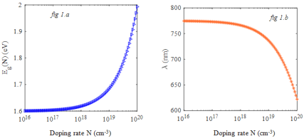
Table 1 summarizes the evolution of the gap energy and wavelength as a function of the doping concentration N.
Table 1. Variation of Eg, N and .
| | | | | |
Eg (eV) | 1.705 | 1.709 | 1.725 | 1.772 | 1.923 |
| 727.4 | 725.3 | 719.04 | 699.7 | 644.9 |
Table 1 shows the variation in bandgap energy and cutoff wavelength as a function of the doping level.
As observed, increasing the doping concentration leads to an apparent widening of the optical bandgap, attributed to the Burstein–Moss effect. This shift results in a blue shift of the absorption edge, meaning the cutoff wavelength moves toward shorter wavelengths.
To better visualize the evolution of optical parameters as a function of doping, the following plots (
Figure 1a and
Figure 1b) provide a graphical representation of the data presented in
Table 1. The first figure shows the variation of the bandgap energy Eg(N), while the second illustrates the evolution of the cutoff wavelength λ(N) with respect to the carrier concentration.
Figure 1. Bandgap energy (Figure 1.a) and cutoff wavelength (Figure 1.b) as a function of doping.
The plots confirm that increasing the doping concentration leads to a widening of the optical bandgap Eg (
Figure 1a), accompanied by a blue shift, as indicated by the decrease in the cutoff wavelength λ (
Figure 1b). This behavior, attributed to the Burstein–Moss effect, demonstrates that doping can be used to tune the material’s spectral response, although careful optimization is required to avoid compromising overall device performance.
2.2. Absorption Coefficient
The absorption coefficient of the InₓGa₁₋ₓN alloy is influenced by several factors, including the molar composition (), temperature, doping level (N), and the wavelength of the incident light. Its expression depends strongly on the composition xxx, with a nonlinear relationship. Moreover, studies have shown that all group III-nitride materials in the wurtzite phase exhibit a direct bandgap, which is favorable for efficient light absorption.
The expression for the absorption coefficient α\alphaα, accounting for the dependence on photon energy, doping, and composition, is derived from the model proposed in
| [17] | V. Chandra, A. D. D. Dwivedi, and N. Sinha. TCAD-based performance assessment of Indium Gallium Nitride based single junction solar cells for different mole fractions of Indium. Optical and Quantum Electronics. 2021, vol. 53, article 72. https://doi.org/10.1007/s11082-020-02709-7 |
| [18] | G. F. Brown, J. W. Ager, W. Walukiewicz, and J. Wu. Finite element simulations of compositionally graded InGaN solar cells. Solar Energy Materials and Solar Cells. 2010, vol. 94, no. 3, pp. 478–483. https://doi.org/10.1016/j.solmat.2009.11.010 |
| [19] | Fickou, F., Camara, M., Thiame, M., Faye, I., Diatta, L. and Faye, M. Modelling and Optimization of the Electrical Parameters of an InxGa1-xN Solar Cell Under. 7th International Conference, InterSol 2024 Dakar, Senegal. pp. 38–46, https://doi.org/10.1007/978-3-031-86493-3_4 |
[17-19]
and is given as:
(5)
Eph is the photon energy (in eV), dependent on the wavelength, is the bandgap energy modified by composition and doping, C(x) and D(x) are composition-dependent parameters, given by:
(6)
(7)
2.3. Refractive Index
In this section, we investigate the influence of the absorber layer thickness and doping concentration on the refractive index of InₓGa₁₋ₓN.
The refractive index n is calculated using the Adachi model, given by the following expression
| [20] | S. Adachi. Refractive indices of III–V compounds: Key properties of InGaAsP relevant to device design. Journal of Applied Physics. 1982, vol. 53, no. 8, pp. 5863–5869. https://doi.org/10.1063/1.331425 |
[20]
:
(8)
Where A and B are empirical parameters dependent on the indium content.
For the InGaN alloy, these parameters are determined through linear interpolation between the values for InN and GaN
| [20] | S. Adachi. Refractive indices of III–V compounds: Key properties of InGaAsP relevant to device design. Journal of Applied Physics. 1982, vol. 53, no. 8, pp. 5863–5869. https://doi.org/10.1063/1.331425 |
[20]
:
(9)
and
(10)
3. Results and Discussion
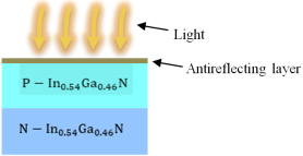
Our reference structure is shown in
Figure 2. It is a single-junction solar cell structure
| [7] | A. Mesrane, F. Rahmoune, A. Mahrane, and A. Oulebsir. Design and simulation of InGaN p–n junction solar cell. International Journal of Photoenergy. 2015, vol. 2015, Article ID 594858, 9 pages. https://doi.org/10.1155/2015/594858 |
[7]
based on
. It consists of: An antireflection coating, deposited on the surface to minimize optical losses due to reflection and to increase the photon flux entering the cell.
Figure 2. Structure of a single-junction InGaN solar cell.
The active P-N layers: the P-layer represents the absorbing region, doped with P-type impurities, and is responsible for carrier generation and collection under illumination. The N-layer forms the N-type region, which, together with the P-layer, establishes the P–N junction that enables the separation of photogenerated carriers (electrons and holes).
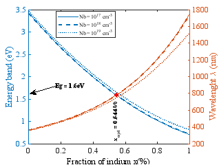
We analyze the evolution of the bandgap energy (Eg) and the cutoff wavelength of the InₓGa₁₋ₓN material as a function of the absorber layer thickness, under different doping conditions. The objective is to explore several alloy compositions (various values of x) in order to identify the optimal configuration that provides a bandgap well-suited for maximum absorption of the solar spectrum. This approach allows for evaluating different InₓGa₁₋ₓN compositions to determine the bandgap that offers the best compromise for solar energy conversion.
Figure 3. Bandgap energy and cutoff wavelength as a function of molar composition x.
The
Figure 3 shows the evolution of the bandgap energy Eg and the cutoff wavelength λ as a function of the indium molar fraction x, for different doping levels. It highlights an inverse correlation between Eg and λ, as well as the influence of doping on the bandgap widening (Burstein–Moss effect). The optimal point xopt=0.54 corresponds to a bandgap of 1.6 eV, which is ideal for maximizing solar spectrum absorption, making it a key parameter for optimizing InGaN solar cells.
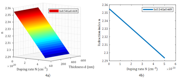
Figure 4 shows the modeling of the refractive index of InₓGa₁₋ₓN as a function of doping concentration and layer thickness. This modeling helps to understand how these parameters affect the optical behavior of the material, particularly the light propagation within the solar cell.
Figure 4. (4a) Variation of the refractive index n as a function of the doping rate N and thickness d for the alloy and (4b) Variation of n as a function of N for a thickness.
and
The simulation results show that the refractive index decreases with increasing doping concentration. However, the effect of doping remains modest for doping levels below . From to , the refractive index can drop significantly. This behavior reflects the plasmonic response of free electrons (Drude model) as well as the reduction in the density of available states for optical absorption (Burstein-Moss effect). This affects the absorption rate of solar cells.
In
Figure 4a, the graph shows that doping has a strong influence on the optical index of In
0.54Ga
0.46N, unlike the layer thickness. This information is crucial for the design of solar cells or optoelectronic devices, as it enables the tuning of optical properties through doping, while the thickness can be adjusted for other purposes (absorption, transport, etc.).
This variation in refractive index with doping directly influences the optical properties of the material, particularly the transmittance (
Figure 5), which must be analyzed to evaluate the solar cell's efficiency. The spectral transmittance
, which describes the fraction of light transmitted through the material, is expressed by the following relationship:
(11)
Where is the reflection coefficient and is the optical absorption coefficient.
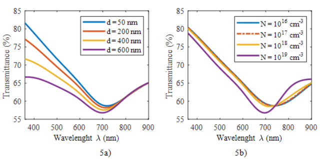
Figure 5. Transmittance as a function of wavelength for different thicknesses (5a) and doping Levels (5b) with .
The transmittance generally decreases with increasing thickness d. The thicker the layer, the more light is absorbed, leading to a reduction in transmittance. This decrease is more pronounced in the spectral region close to the material’s absorption edge. This trend is consistent with the Beer–Lambert absorption law:
In conclusion, a greater thickness improves absorption (beneficial for photocurrent generation), but reduces transmittance, which could be detrimental for tandem cell structures. Excessive doping degrades transmittance, especially in the infrared (IR) region, due to free carrier absorption and spectral shifting. Therefore, optimization involves finding a trade-off: a thickness sufficient to ensure effective absorption, and a moderate doping level to limit optical losses while maintaining good electrical conductivity.
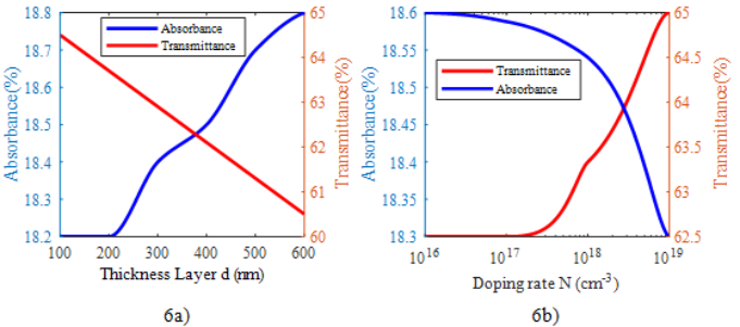
Following the analysis of transmittance, which helps evaluate the optical losses due to light passing through the material, it is essential to examine the absorbance in order to quantify the efficiency of photon absorption directly linked to carrier generation in the InGaN solar cell (
Figure 6).
The analysis of absorbance emerges as a complementary step to that of transmittance, as it allows the estimation of the fraction of light energy effectively absorbed by the active layer.
Figure 6. Absorbance and Transmittance as a Function of Layer Thickness (a) and Doping Level (b) with .
Figure 6a and 6b above illustrate the joint evolution of the absorbance and transmittance of the InGaN material as a function of the thickness of the absorbing layer (6a) and the doping level N (6b).
The analysis (
Figure 6a) shows that the absorbance increases slightly with thickness, from 18.3% (100 nm) to 18.8% (600 nm), while the transmittance decreases almost linearly from 65% to 60%, in accordance with Beer–Lambert's law. The optimal thickness is between 300 and 400 nm, maximizing absorption while limiting optical losses.
Regarding doping (
Figure 6b), a low concentration (≈10
16 cm
-3) results in maximum transmittance (~65%) and minimum absorbance (~18.3%). Absorbance reaches a maximum (~18.6%) at around 10
12 cm
-3 before decreasing at high doping levels, due to the Burstein–Moss effect and free carrier scattering.
Therefore, a thickness of approximately 500 nm and doping between 10
17 and 10
12 cm
-3 constitute an optimal compromise for maximizing photovoltaic performance, in agreement with the findings reported by Mesrane et al.
| [7] | A. Mesrane, F. Rahmoune, A. Mahrane, and A. Oulebsir. Design and simulation of InGaN p–n junction solar cell. International Journal of Photoenergy. 2015, vol. 2015, Article ID 594858, 9 pages. https://doi.org/10.1155/2015/594858 |
[7]
.
The use of piecewise cubic Hermite interpolation (PCHIP) made it possible to obtain transmittance and absorbance models as a function of layer thickness.
with
(15)
with
These models confirm the trend observed experimentally and enable the optical behavior to be predicted for any intermediate thickness.
To support the previous analyses, the following tables present numerical values of absorbance, transmittance, and external quantum efficiency (EQE) as functions of the active layer thickness (
Table 2) and doping level N (
Table 3), for different wavelengths. These data allow a more precise evaluation of the impact of these parameters on the optoelectronic behavior of InGaN material.
Table 2. Values of Absorbance, Transmittance, and External Quantum Efficiency (EQE) as a Function of Layer Thickness d.
| | | EQE (%) |
50 | 13.6 | 18.2 | 18.8 | 17.1 | 82.1 | 64.9 | 58.9 | 61.1 | 97.3 | 92.8 | 87.5 |
100 | 13.8 | 18.2 | 18.9 | 17.1 | 81.4 | 64.5 | 58.7 | 61.1 | 97.3 | 92.8 | 87.5 |
200 | 14.2 | 18.4 | 18.9 | 17.1 | 79.9 | 63.7 | 58.3 | 61.1 | 97.3 | 92.8 | 87.5 |
300 | 14.6 | 18.5 | 19 | 17.1 | 78.5 | 62.9 | 58 | 61.1 | 97.3 | 92.8 | 87.5 |
400 | 15 | 18.7 | 19.1 | 17.1 | 77.1 | 62.1 | 57.6 | 61.1 | 97.3 | 92.8 | 87.5 |
500 | 15.5 | 18.8 | 19.2 | 17.1 | 75.7 | 61.3 | 57.2 | 61.1 | 97.3 | 92.8 | 87.5 |
600 | 15.9 | 19 | 19.3 | 17.1 | 74.3 | 60.5 | 56.8 | 61.1 | 97.3 | 92.8 | 87.5 |
| 360 | 600 | 700 | 800 | 360 | 600 | 700 | 800 | 360 | 600 | 700 |
Table 3. Values of Absorbance, Transmittance, and External Quantum Efficiency (EQE) as a Function of Doping Level N.
| | | EQE (%) |
| 14 | 18.3 | 18.9 | 17.4 | 80.4 | 65 | 59.3 | 60 | 97.7 | 93.7 | 89 |
| 14.1 | 18.3 | 18.9 | 17.4 | 80.3 | 64.9 | 59.2 | 60.2 | 97.3 | 92.8 | 87.5 |
| 14.2 | 18.4 | 18.9 | 17.1 | 80.1 | 64.5 | 58.7 | 61.1 | 96.1 | 89.6 | 81.8 |
| 14.8 | 18.6 | 19.1 | 16.2 | 78.8 | 62.5 | 56.8 | 63.5 | 91.9 | 78.1 | 58.2 |
| 360 | 600 | 700 | 800 | 360 | 600 | 700 | 800 | 360 | 600 | 700 |
These numerical results highlight the sensitivity of the optical response of InGaN material to physical design parameters. While increasing the layer thickness enhances absorption without significantly impairing performance, excessive doping, on the other hand, leads to a marked degradation in both transmittance and external quantum efficiency (EQE).
Thus, optimizing an InGaN solar cell requires a trade-off between thickness and doping: an active layer thickness between 300 and 500 nm, combined with a doping level in the range of to , appears to be the most favorable configuration for achieving efficient photon absorption and effective carrier collection.
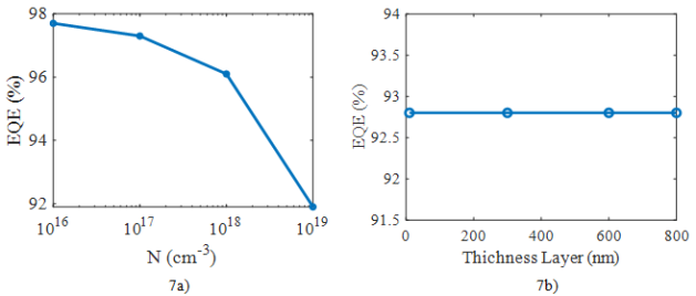
To better visualize the quantitative impact of doping and thickness on external quantum efficiency, the following graphs illustrate the evolution of EQE as a function of doping level N (left) and active layer thickness (right). These graphical representations visually confirm the trends observed in the previous tables.
Figure 7. External Quantum Efficiency as a Function of Doping Level (7a) and Layer Thickness (7b).
The two graphs clearly and succinctly confirm the distinct effects of doping and thickness on the optical performance of the InGaN cell.
In
Figure 7a, a significant decrease in EQE is observed as doping increases, particularly beyond 10
12 cm
-3. This trend highlights the negative influence of high doping levels on the collection of photogenerated carriers, due to non-radiative recombination and free carrier absorption losses.
In
Figure 7b, the variation in EQE as a function of thickness is negligible within the considered range (up to 700 nm), indicating that absorbance is already sufficient at low thickness to ensure excellent carrier collection. This confirms that, under certain spectral conditions, increasing the thickness does not provide any significant improvement in external quantum efficiency.
These results underline the importance of controlling the doping level to optimize the performance of InGaN-based solar cells, while the thickness can be adjusted more flexibly without compromising the overall optoelectronic efficiency.
Our results fall within the range of previously published performances:
Nor Bochra et al.
studied the characterization of InGaN solar cells and highlighted the high potential of this material for photovoltaic applications.
Benmoussa et al.
| [22] | D. Benmoussa. Simulation of In0.52Ga0.48N solar cell using AMPS-1D", in Proceedings of the 1st international Renewable and Sustainable Energie Conference (IRSEC'13), March 2013, pp. 23-26, IEEE, Ouarzazate, Morocco. |
[22]
reported an efficiency of 22.99% for an In
0.52Ga
0.48N solar cell simulated using AMPS-1D, with layer thicknesses of 600 nm (P) and 230 nm (N), and a doping concentration of 10
15 cm
-3.
These comparisons demonstrate that our simulation results are consistent with the expected performance range of InGaN solar cells.
Author Contributions
Sada Traore: Data curation, Formal Analysis, Funding acquisition, Methodology, Project administration, Supervision, Validation, Visualization, Writing – review & editing
Baboucar Fickou: Conceptualization, Formal Analysis, Funding acquisition, Project administration, Resources, Supervision, Validation, Visualization, Writing – review & editing
Moustapha Thiame: Conceptualization, Data curation, Funding acquisition, Investigation, Project administration, Resources, Software, Visualization, Writing – original draft
Modou Tine: Conceptualization, Data curation, Funding acquisition, Investigation, Project administration, Resources, Software, Visualization, Writing – original draft